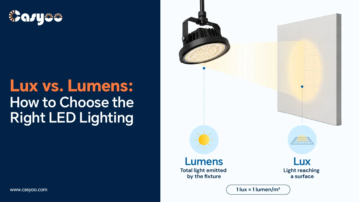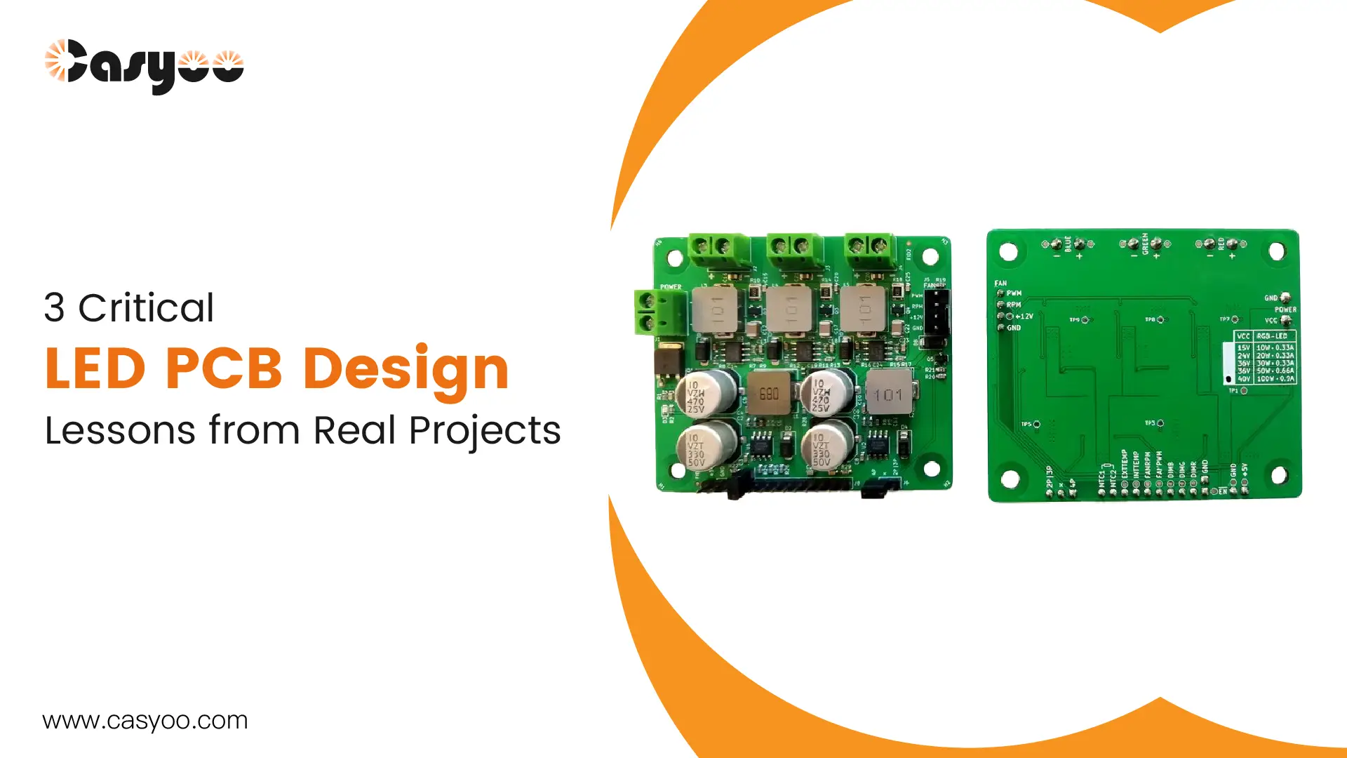
What are the most crucial points of LED PCB board design? A long-term LED light necessities efficient thermal management, accurate driving/current control and an optimized layout. In this in-depth LED PCB design guide, we’re going in detail into these three most significant pillars of great LED PCB design, and share real-world best practices that can enable you to engineer truly superior LED products. Read and learn more!
Lesson 1: Thermal Management in LED PCB Design
Though LEDs are ultra-efficient, a small amount of the energy they consume is converted to heat at the junction. When this heat accumulates, the actual temperature within the LED, or junction temperature (Tj) will soar. Elevated Tj soon results in less light, strange color changes, and eventually, a significantly shorter lifespan for your LEDs.
Our primary goal in LED light circuit board design for thermal management is to provide a clear efficient path for the heat to get out of the LED chip, travel through the PCB and into the air surrounding it. This includes consideration of what is used, the construction of things and even how they are assembled.
The following are some practical examples illustrating the superior methods of managing the heat in the design of IPC LED PCB:
Case Study 1: The Robustness of Aluminum Substrates in LED Streetlights
Consistent heat control is the key when you have large and long-term projects in place such as highway tunnel lightings. Standard FR-4 type PCBs can not handle the heat these set-ups throw off.
Take one project that used an aluminum substrate (specifically 6061 aluminum alloy): after three years of running full tilt for about 12 hours a day, the light only dimmed by a tiny 12%. That compared to a 35 percent decline in a typical FR-4 setup. This difference clearly shows how vital the right PCB material is for making LEDs last.
The secret was a thick 1.5mm aluminum core (180-200 W/(m·K) thermal conductivity) with a super thin (80μm) yet robust (1.5 W/(m·K)) ceramic-filled epoxy insulation, plus an anodized surface for better heat radiation and a combined cooling fin/natural convection design that slashed thermal resistance to just 0.8°C/W.
Case Study 2: Innovative Thermo-Electric Separation in High-Power LED Color Modules
The standard aluminum substrate may not suffice, particularly high-power applications, where the LED color modules are extremely demanding. The real challenge is getting heat away from the LED chip directly to the heat sink without any electrical interference. One high-power LED color module project came up with a clever thermo-electric separation structure, where the metal bumps for the LED chips were built right into the baseplate. That clever design reduced the junction temperature by 20°C and increased light output by 15% over aged copper-based PCBs.
They achieved this by having separate copper layers for circuits and heat, with the heat layer directly under the LED chip for an ultra-low thermal resistance of 0.5°C/W, using highly conductive copper pedestals (401 W/(m·K)) on a 6061 aluminum alloy base, and a very thin (50μm) ceramic-filled insulation layer (3 W/(m·K)), ultimately lowering the operating temperature from 140°C to just 100°C.
Lesson 2: Driving and Current Control in LED PCB Design
Effective LED driver circuit does more than merely powering it. It effectively controls the voltage variations, optimizes power conversion and offers essential protection capabilities. Such circuits may use a range of topologies such as buck (step-down), boost (step-up), or buck-boost (step-up/step-down) to suit the input voltages and the LED string arrangements. The issue is how to make these circuits as efficient and with minimum ripple and strongly guarded against electrical accidents.
The following is a workable representation of an advanced buck-boost driver scheme:
Case Study: A Robust Buck-Boost Driver for 5S2P AR111 LED Lamps

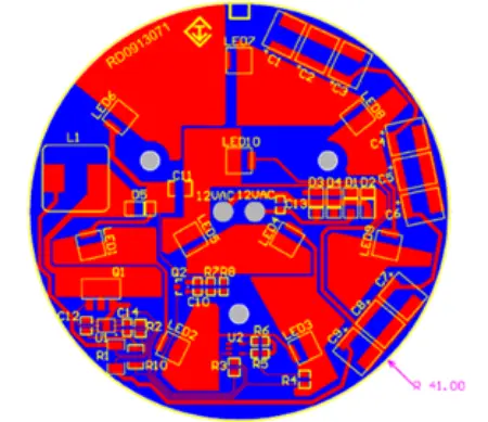
This reference design provides a general purpose buck-boost driving solution to a 5S2P AR111 LED lamp, with a 12VAC +10% input. The circuit is an efficient way of converting AC to smooth DC with flicker requirements balanced against cost. In parallel strings, the design reduces the current mismatch by selecting LEDs with good pairs, and limiting the string number.
The controller is MAX16819, which can be adapted to operate as a buck-boost power source to provide a predictable output at all input voltages over the range of LED string voltages. The choice of an inductor is critical; a 39 uH Coilcraft inductor at rated currents was chosen with the help of calculations, and an 80mΩ sense resistor is used to handle the ripple to the input voltage.
In addition to power, there is strong protection constructed. Protection against catastrophic failure is provided by an overvoltage (OV) protection circuit that clamps output to 30V in case a string is disconnected. There also is the use of foldback thermal management which senses increasing temperatures using an NTC thermistor to automatically dim the LED current to achieve a self-balancing system. This is helpful to lamps with restricted air flow so that they do not fail. The selected MOSFET provides efficiency switch loss.
Lastly, it is the PCB layout of the driver. The top layer has components and a solid ground plane is underneath. Large copper pours improve the transfer of heat to the exterior aluminum structure which then forms an extended heat sink, providing optimal component temperatures.
Lesson 3: Longevity Through LED PCB Layout
The way you design your PCBs layout makes a huge difference to how long an LED will last. This is mainly concerned with prevention of Electrical Overstress (EOS). A good PCB layout with LEDs control the current paths well and eliminate stress points in an environmentally safe system. This means placing components accurately, intelligent trace routing and careful planning of isolation and grounding. Let’s explore LED PCB layout best practices on preventing EOS:
Case Study: Strategic PCB Layout for EOS Prevention
First, clearance and creepage distances are basic. Have enough space between copper and fixture material by about 3-7mm. For screw placements, base clearances on the screw head diameter. By soldering wires directly together with insulation, it is vital to ensure that all cable insulation covers the solder pads in order to maintain creepage distance. The dielectric used in aluminum-base PCBs, has to match easy heat transfer with enough electrical isolation; be sure your supplier guarantees breakdown voltage.
It is also essential to deal with common and differential mode surges. Do not leave any LED thermal pads floating electrically; tie each to a common voltage reference, and all of the thermal pads to each other in order to shunt any surge energy. The best layout is a “mirrored” symmetrical layout with positive-side pads tied to anode with negative-side to cathode to provide comprehensive surge protection. This protection can also be further increased by additional capacitors (CP/CN), and grounding the fixture body to power output terminals (as allowed according to IEC 60598-1:2014) can reduce EOS as well.

Designers can essentially mitigate LEDs against EOS by carefully using these layout best practices, such as: clearance considerations, strong dielectric capabilities and a well-placed set of thermal pads.
Common Mistakes in LED PCB Design
Inadequate Thermal Management
Failure to observe good thermal dissipation is one of the commonest traps in LED PCB design. The LEDs produce much heat, particularly large-power LEDs, and inadequate heat aid or thermal via may lead to poor lasting and execution.
Solution:
The PCB layout should include thermal vias, aluminum substrates and/or heat sinks to maintain an even distribution of heat and support the life of the LED.
Insufficient Current Control
Designers occasionally disregard the significance of steady current controller. Driving LEDs without proper current-limiting components can lead to overheating, color shifting, or premature failure.
Solution:
Always incorporate high quality current limiting resistors or constant current driver circuit to ensure safe repeatable operation of the LED.
Poor Trace Sizing and Layout
Another common problem is using secondary traces that are not wide enough to accommodate needed current load. This may result in voltage drops, local hot-spots or even burn-outs in time, especially when used in high-brightness light.
Solution:
Compute trace width using the anticipated current and specification of PCB material, and use short, wide routing of the power lines to reduce resistance and maximize efficiency.
Still experiencing difficulties?
Why not consult an LED maker that is accustomed to LED PCB design? Casyoo has delivered over 10 million custom LED PCBs for clients in horticulture, street lighting, and industrial applications. Explore Our LED PCB Design Service from now on!